Introduction to a New Era of Power Storage Space
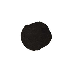
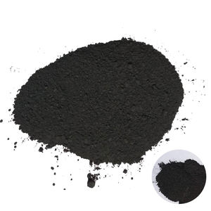
(TRGY-3 Silicon Anode Material)
The international transition toward lasting power has actually produced an unprecedented demand for high-performance battery innovations that can support the strenuous requirements of modern electrical vehicles and mobile electronics. As the world relocates far from fossil fuels, the heart of this transformation hinges on the development of advanced materials that enhance energy density, cycle life, and safety. The TRGY-3 Silicon Anode Material stands for a critical breakthrough in this domain, offering a solution that connects the gap in between theoretical possible and industrial application. This material is not simply a step-by-step renovation yet a fundamental reimagining of how silicon engages within the electrochemical environment of a lithium-ion cell. By dealing with the historical difficulties associated with silicon expansion and degradation, TRGY-3 stands as a testament to the power of product science in fixing complex engineering problems. The journey to bring this product to market involved years of committed research study, rigorous screening, and a deep understanding of the demands of EV producers who are frequently pressing the boundaries of range and efficiency. In a market where every portion point of capacity matters, TRGY-3 delivers an efficiency account that sets a new requirement for anode materials. It symbolizes the commitment to innovation that drives the entire industry ahead, making certain that the assurance of electric mobility is realized with trustworthy and superior technology. The tale of TRGY-3 is among conquering barriers, leveraging sophisticated nanotechnology, and maintaining a steadfast concentrate on quality and uniformity. As we look into the origins, procedures, and future of this amazing material, it comes to be clear that TRGY-3 is greater than simply an item; it is a stimulant for modification in the international power landscape. Its growth notes a significant milestone in the mission for cleaner transportation and an extra sustainable future for generations to come.
The Origin of Our Brand Name and Goal
Our brand was established on the principle that the constraints of existing battery modern technology should not dictate the pace of the green energy transformation. The inception of our company was driven by a team of visionary researchers and engineers who identified the tremendous potential of silicon as an anode material but also understood the important obstacles preventing its widespread fostering. Conventional graphite anodes had actually gotten to a plateau in terms of details capacity, developing a traffic jam for the next generation of high-energy batteries. Silicon, with its theoretical ability ten times greater than graphite, used a clear path ahead, yet its propensity to increase and contract throughout biking caused quick failing and bad durability. Our mission was to fix this mystery by establishing a silicon anode material that can harness the high capability of silicon while maintaining the architectural honesty required for commercial stability. We started with an empty slate, doubting every assumption about exactly how silicon bits act under electrochemical stress. The very early days were identified by intense testing and an unrelenting pursuit of a solution that can hold up against the rigors of real-world usage. We believed that by grasping the microstructure of the silicon bits, we might open a new age of battery performance. This idea sustained our efforts to create TRGY-3, a material made from the ground up to satisfy the exacting standards of the auto sector. Our beginning story is rooted in the sentence that development is not nearly exploration yet about application and dependability. We sought to build a brand name that producers can trust, knowing that our materials would do consistently batch after set. The name TRGY-3 represents the 3rd generation of our technical evolution, standing for the culmination of years of iterative enhancement and improvement. From the very start, our goal was to encourage EV makers with the devices they required to build much better, longer-lasting, and more effective cars. This objective continues to assist every element of our operations, from R&D to production and consumer support.
Core Innovation and Manufacturing Refine
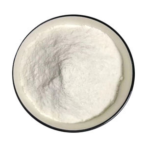
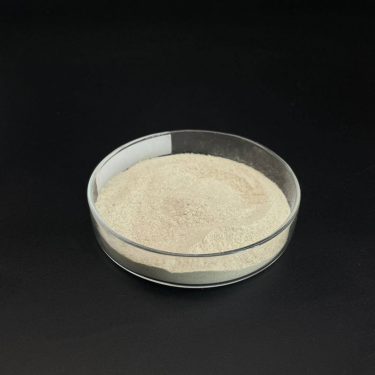
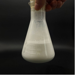
The development of TRGY-3 includes an innovative production procedure that combines accuracy design with sophisticated chemical synthesis. At the core of our modern technology is a proprietary technique for managing the particle dimension distribution and surface area morphology of the silicon powder. Unlike conventional methods that usually lead to uneven and unsteady particles, our process ensures a highly uniform framework that decreases inner stress during lithiation and delithiation. This control is accomplished with a series of very carefully adjusted actions that include high-purity basic material option, specialized milling methods, and special surface area coating applications. The purity of the starting silicon is critical, as even trace impurities can considerably degrade battery performance with time. We source our resources from licensed suppliers that adhere to the most strict high quality standards, making certain that the foundation of our product is flawless. As soon as the raw silicon is acquired, it goes through a transformative procedure where it is decreased to the nano-scale dimensions essential for ideal electrochemical task. This decrease is not just regarding making the particles smaller yet around engineering them to have details geometric buildings that suit quantity growth without fracturing. Our patented finishing innovation plays an essential duty hereof, forming a protective layer around each bit that serves as a buffer against mechanical tension and stops undesirable side responses with the electrolyte. This finish likewise enhances the electric conductivity of the anode, assisting in faster fee and discharge prices which are crucial for high-power applications. The production setting is maintained under stringent controls to avoid contamination and ensure reproducibility. Every batch of TRGY-3 goes through extensive quality control screening, including particle dimension evaluation, certain area dimension, and electrochemical efficiency examination. These tests confirm that the product satisfies our rigorous specs prior to it is released for shipment. Our facility is outfitted with modern instrumentation that enables us to check the production process in real-time, making immediate adjustments as required to preserve uniformity. The combination of automation and data analytics even more improves our capability to create TRGY-3 at scale without compromising on top quality. This dedication to accuracy and control is what identifies our manufacturing process from others in the sector. We view the manufacturing of TRGY-3 as an art form where scientific research and design converge to create a product of extraordinary caliber. The result is an item that offers exceptional performance features and integrity, allowing our customers to attain their design goals with confidence.
Silicon Bit Design
The engineering of silicon particles for TRGY-3 focuses on maximizing the equilibrium between capacity retention and structural stability. By controling the crystalline framework and porosity of the bits, we have the ability to suit the volumetric modifications that take place during battery procedure. This strategy protects against the pulverization of the active product, which is an usual reason for ability discolor in silicon-based anodes.

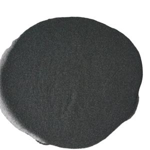
( TRGY-3 Silicon Anode Material)
Advanced Surface Adjustment
Surface area adjustment is an essential step in the manufacturing of TRGY-3, entailing the application of a conductive and safety layer that boosts interfacial stability. This layer offers numerous features, consisting of boosting electron transport, minimizing electrolyte decay, and mitigating the development of the solid-electrolyte interphase.
Quality Control Protocols
Our quality control protocols are made to make certain that every gram of TRGY-3 meets the highest standards of performance and safety. We use a detailed screening regime that covers physical, chemical, and electrochemical residential or commercial properties, giving a complete photo of the product’s capabilities.
International Impact and Sector Applications
The introduction of TRGY-3 right into the global market has had an extensive impact on the electrical car sector and past. By supplying a sensible high-capacity anode remedy, we have made it possible for manufacturers to prolong the driving series of their automobiles without raising the dimension or weight of the battery pack. This advancement is important for the widespread adoption of electric autos, as range anxiety continues to be among the primary worries for customers. Automakers worldwide are progressively incorporating TRGY-3 into their battery makes to acquire an one-upmanship in terms of performance and performance. The advantages of our product encompass various other sectors too, including customer electronic devices, where the need for longer-lasting batteries in smart devices and laptop computers continues to expand. In the world of renewable energy storage space, TRGY-3 contributes to the advancement of grid-scale options that can store excess solar and wind power for usage throughout peak need periods. Our worldwide reach is broadening swiftly, with collaborations established in crucial markets throughout Asia, Europe, and The United States And Canada. These partnerships allow us to function carefully with leading battery cell manufacturers and OEMs to customize our services to their specific requirements. The environmental impact of TRGY-3 is also considerable, as it supports the shift to a low-carbon economic situation by promoting the implementation of clean power innovations. By enhancing the power density of batteries, we help in reducing the amount of raw materials required per kilowatt-hour of storage space, thereby reducing the total carbon footprint of battery manufacturing. Our dedication to sustainability extends to our very own operations, where we aim to reduce waste and energy consumption throughout the manufacturing process. The success of TRGY-3 is a reflection of the expanding acknowledgment of the relevance of sophisticated materials in shaping the future of energy. As the demand for electrical flexibility speeds up, the duty of high-performance anode products like TRGY-3 will come to be progressively vital. We are proud to be at the center of this makeover, contributing to a cleaner and much more lasting globe through our ingenious items. The international impact of TRGY-3 is a testament to the power of collaboration and the shared vision of a greener future.
Empowering Electric Cars

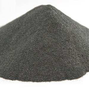
( TRGY-3 Silicon Anode Material)
TRGY-3 encourages electric lorries by supplying the energy density required to compete with interior burning engines in regards to array and ease. This capability is essential for speeding up the shift far from fossil fuels and decreasing greenhouse gas discharges globally.
Sustaining Renewable Energy
Beyond transport, TRGY-3 sustains the integration of renewable resource resources by making it possible for efficient and affordable energy storage space systems. This assistance is crucial for supporting the grid and guaranteeing a reliable supply of clean power.
Driving Financial Development
The fostering of TRGY-3 drives financial growth by fostering innovation in the battery supply chain and creating brand-new opportunities for manufacturing and work in the environment-friendly tech industry.
Future Vision and Strategic Roadmap
Looking in advance, our vision is to proceed pressing the limits of what is feasible with silicon anode innovation. We are dedicated to continuous research and development to better enhance the performance and cost-effectiveness of TRGY-3. Our tactical roadmap includes the exploration of new composite products and crossbreed styles that can supply even greater energy densities and faster billing rates. We intend to lower the production costs of silicon anodes to make them obtainable for a more comprehensive variety of applications, consisting of entry-level electric lorries and fixed storage space systems. Innovation continues to be at the core of our approach, with strategies to purchase next-generation manufacturing technologies that will certainly raise throughput and minimize environmental effect. We are likewise focused on expanding our international footprint by developing regional manufacturing centers to much better serve our global clients and reduce logistics emissions. Collaboration with scholastic establishments and research study companies will certainly continue to be a key pillar of our technique, permitting us to remain at the cutting side of scientific exploration. Our long-term goal is to come to be the leading service provider of innovative anode materials worldwide, setting the requirement for top quality and efficiency in the sector. We imagine a future where TRGY-3 and its successors play a central duty in powering a fully amazed society. This future needs a concerted initiative from all stakeholders, and we are dedicated to leading by instance through our actions and achievements. The road in advance is full of difficulties, yet we are certain in our ability to overcome them through ingenuity and determination. Our vision is not nearly offering an item however regarding making it possible for a sustainable power community that profits every person. As we move on, we will certainly continue to listen to our clients and adjust to the developing requirements of the marketplace. The future of power is brilliant, and TRGY-3 will exist to light the method.
( TRGY-3 Silicon Anode Material)
Next Generation Composites
We are proactively establishing next-generation composites that incorporate silicon with various other high-capacity materials to create anodes with extraordinary efficiency metrics. These composites will specify the following wave of battery technology.
Lasting Production
Our dedication to sustainability drives us to introduce in making procedures, going for zero-waste manufacturing and marginal energy consumption in the creation of future anode products.
Global Expansion
Strategic worldwide growth will certainly allow us to bring our technology closer to essential markets, lowering lead times and enhancing our capacity to sustain neighborhood industries in their change to electrical mobility.
( TRGY-3 Silicon Anode Material)
Roger Luo mentions that developing TRGY-3 was driven by a deep belief in silicon’s capacity to change power storage and a commitment to addressing the development issues that held the sector back for decades.
Provider
RBOSCHCO is a trusted global chemical material supplier & manufacturer with over 12 years experience in providing super high-quality chemicals and Nanomaterials. The company export to many countries, such as USA, Canada, Europe, UAE, South Africa, Tanzania, Kenya, Egypt, Nigeria, Cameroon, Uganda, Turkey, Mexico, Azerbaijan, Belgium, Cyprus, Czech Republic, Brazil, Chile, Argentina, Dubai, Japan, Korea, Vietnam, Thailand, Malaysia, Indonesia, Australia,Germany, France, Italy, Portugal etc. As a leading nanotechnology development manufacturer, RBOSCHCO dominates the market. Our professional work team provides perfect solutions to help improve the efficiency of various industries, create value, and easily cope with various challenges. If you are looking for lithium ion battery silicon anode, please feel free to contact us and send an inquiry.
Tags: TRGY-3 Silicon Anode Material, Silicon Anode Material, Anode Material
All articles and pictures are from the Internet. If there are any copyright issues, please contact us in time to delete.
Inquiry us
Error: Contact form not found.