1. hemical Nature and Architectural Characteristics
1.1 Molecular Composition and Self-Assembly Behavior

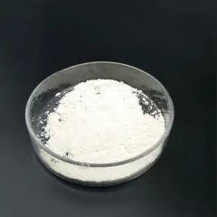
(Calcium Stearate Powder)
Calcium stearate powder is a metallic soap formed by the neutralization of stearic acid– a C18 saturated fatty acid– with calcium hydroxide or calcium oxide, producing the chemical formula Ca(C ₁₈ H ₃₅ O TWO)TWO.
This substance belongs to the broader course of alkali earth steel soaps, which display amphiphilic residential or commercial properties as a result of their twin molecular architecture: a polar, ionic “head” (the calcium ion) and two long, nonpolar hydrocarbon “tails” originated from stearic acid chains.
In the solid state, these molecules self-assemble into layered lamellar frameworks via van der Waals interactions between the hydrophobic tails, while the ionic calcium facilities supply structural communication using electrostatic pressures.
This unique setup underpins its capability as both a water-repellent agent and a lubricant, allowing performance across varied product systems.
The crystalline kind of calcium stearate is normally monoclinic or triclinic, depending upon processing problems, and exhibits thermal security as much as about 150– 200 ° C prior to decay begins.
Its reduced solubility in water and most organic solvents makes it especially appropriate for applications requiring consistent surface area alteration without leaching.
1.2 Synthesis Paths and Industrial Production Approaches
Commercially, calcium stearate is produced by means of 2 main courses: direct saponification and metathesis response.
In the saponification procedure, stearic acid is responded with calcium hydroxide in a liquid tool under controlled temperature (normally 80– 100 ° C), complied with by purification, washing, and spray drying to generate a fine, free-flowing powder.
Conversely, metathesis includes responding salt stearate with a soluble calcium salt such as calcium chloride, speeding up calcium stearate while creating sodium chloride as a by-product, which is after that eliminated with comprehensive rinsing.
The choice of technique influences bit size circulation, purity, and residual dampness material– crucial specifications influencing efficiency in end-use applications.
High-purity grades, specifically those intended for drugs or food-contact products, go through additional purification steps to fulfill governing requirements such as FCC (Food Chemicals Codex) or USP (USA Pharmacopeia).
( Calcium Stearate Powder)
Modern production centers employ continual activators and automated drying out systems to make sure batch-to-batch uniformity and scalability.
2. Practical Functions and Systems in Material Equipment
2.1 Internal and External Lubrication in Polymer Processing
One of the most crucial features of calcium stearate is as a multifunctional lubricating substance in polycarbonate and thermoset polymer manufacturing.
As an interior lube, it minimizes thaw thickness by interfering with intermolecular rubbing in between polymer chains, facilitating less complicated circulation during extrusion, shot molding, and calendaring procedures.
At the same time, as an outside lube, it moves to the surface area of liquified polymers and creates a thin, release-promoting movie at the user interface between the product and handling devices.
This dual action reduces pass away accumulation, stops sticking to mold and mildews, and boosts surface finish, thus enhancing manufacturing efficiency and product quality.
Its performance is especially noteworthy in polyvinyl chloride (PVC), where it likewise adds to thermal stability by scavenging hydrogen chloride launched during destruction.
Unlike some synthetic lubricants, calcium stearate is thermally steady within typical processing home windows and does not volatilize prematurely, making sure regular performance throughout the cycle.
2.2 Water Repellency and Anti-Caking Features
Due to its hydrophobic nature, calcium stearate is widely employed as a waterproofing agent in construction products such as cement, plaster, and plasters.
When included into these matrices, it lines up at pore surfaces, reducing capillary absorption and improving resistance to moisture access without substantially modifying mechanical toughness.
In powdered items– consisting of plant foods, food powders, drugs, and pigments– it serves as an anti-caking agent by coating specific particles and preventing cluster triggered by humidity-induced linking.
This boosts flowability, managing, and application accuracy, specifically in automated product packaging and mixing systems.
The device counts on the formation of a physical obstacle that prevents hygroscopic uptake and decreases interparticle bond forces.
Due to the fact that it is chemically inert under normal storage problems, it does not react with energetic components, protecting shelf life and capability.
3. Application Domains Across Industries
3.1 Function in Plastics, Rubber, and Elastomer Production
Past lubrication, calcium stearate functions as a mold and mildew launch representative and acid scavenger in rubber vulcanization and synthetic elastomer production.
During intensifying, it ensures smooth脱模 (demolding) and secures pricey steel dies from corrosion caused by acidic byproducts.
In polyolefins such as polyethylene and polypropylene, it enhances diffusion of fillers like calcium carbonate and talc, contributing to consistent composite morphology.
Its compatibility with a wide range of additives makes it a recommended component in masterbatch solutions.
Moreover, in naturally degradable plastics, where typical lubricants may disrupt deterioration pathways, calcium stearate offers a more environmentally suitable choice.
3.2 Usage in Pharmaceuticals, Cosmetics, and Food Products
In the pharmaceutical market, calcium stearate is generally made use of as a glidant and lube in tablet compression, guaranteeing constant powder circulation and ejection from strikes.
It protects against sticking and topping defects, straight influencing manufacturing return and dosage uniformity.
Although occasionally puzzled with magnesium stearate, calcium stearate is preferred in particular formulations because of its greater thermal stability and reduced potential for bioavailability interference.
In cosmetics, it functions as a bulking representative, structure modifier, and solution stabilizer in powders, foundations, and lipsticks, supplying a smooth, smooth feeling.
As an artificial additive (E470(ii)), it is authorized in several jurisdictions as an anticaking representative in dried out milk, seasonings, and baking powders, adhering to rigorous limits on optimum allowable focus.
Regulative conformity calls for rigorous control over heavy steel web content, microbial load, and recurring solvents.
4. Security, Environmental Effect, and Future Overview
4.1 Toxicological Profile and Regulatory Status
Calcium stearate is normally recognized as secure (GRAS) by the united state FDA when used in accordance with great manufacturing methods.
It is badly soaked up in the gastrointestinal system and is metabolized right into normally occurring fats and calcium ions, both of which are from a physical standpoint manageable.
No significant evidence of carcinogenicity, mutagenicity, or reproductive poisoning has been reported in basic toxicological studies.
Nevertheless, breathing of fine powders during commercial handling can create respiratory irritability, necessitating appropriate ventilation and individual protective equipment.
Ecological influence is very little because of its biodegradability under cardiovascular conditions and reduced marine poisoning.
4.2 Arising Fads and Lasting Alternatives
With enhancing emphasis on green chemistry, research study is concentrating on bio-based production paths and lowered ecological footprint in synthesis.
Efforts are underway to acquire stearic acid from sustainable resources such as palm kernel or tallow, improving lifecycle sustainability.
In addition, nanostructured forms of calcium stearate are being checked out for boosted dispersion effectiveness at reduced does, potentially decreasing total material use.
Functionalization with various other ions or co-processing with natural waxes may broaden its utility in specialty finishings and controlled-release systems.
In conclusion, calcium stearate powder exhibits exactly how a straightforward organometallic compound can play an overmuch huge role throughout industrial, consumer, and health care markets.
Its combination of lubricity, hydrophobicity, chemical security, and regulative acceptability makes it a foundation additive in modern-day formulation science.
As markets continue to require multifunctional, secure, and lasting excipients, calcium stearate remains a benchmark material with enduring significance and evolving applications.
5. Vendor
RBOSCHCO is a trusted global chemical material supplier & manufacturer with over 12 years experience in providing super high-quality chemicals and Nanomaterials. The company export to many countries, such as USA, Canada, Europe, UAE, South Africa, Tanzania, Kenya, Egypt, Nigeria, Cameroon, Uganda, Turkey, Mexico, Azerbaijan, Belgium, Cyprus, Czech Republic, Brazil, Chile, Argentina, Dubai, Japan, Korea, Vietnam, Thailand, Malaysia, Indonesia, Australia,Germany, France, Italy, Portugal etc. As a leading nanotechnology development manufacturer, RBOSCHCO dominates the market. Our professional work team provides perfect solutions to help improve the efficiency of various industries, create value, and easily cope with various challenges. If you are looking for c36h70cao4, please feel free to contact us and send an inquiry.
Tags: Calcium Stearate Powder, calcium stearate,ca stearate
All articles and pictures are from the Internet. If there are any copyright issues, please contact us in time to delete.
Inquiry us
Error: Contact form not found.