1. Product Properties and Structural Honesty
1.1 Inherent Qualities of Silicon Carbide

(Silicon Carbide Crucibles)
Silicon carbide (SiC) is a covalent ceramic compound made up of silicon and carbon atoms set up in a tetrahedral latticework structure, mainly existing in over 250 polytypic kinds, with 6H, 4H, and 3C being the most highly appropriate.
Its solid directional bonding imparts extraordinary solidity (Mohs ~ 9.5), high thermal conductivity (80– 120 W/(m · K )for pure single crystals), and exceptional chemical inertness, making it one of one of the most robust products for extreme settings.
The wide bandgap (2.9– 3.3 eV) guarantees exceptional electrical insulation at area temperature and high resistance to radiation damage, while its reduced thermal expansion coefficient (~ 4.0 × 10 ⁻⁶/ K) contributes to superior thermal shock resistance.
These intrinsic homes are preserved even at temperature levels exceeding 1600 ° C, permitting SiC to maintain structural stability under long term exposure to molten steels, slags, and responsive gases.
Unlike oxide porcelains such as alumina, SiC does not respond conveniently with carbon or type low-melting eutectics in lowering atmospheres, a critical benefit in metallurgical and semiconductor handling.
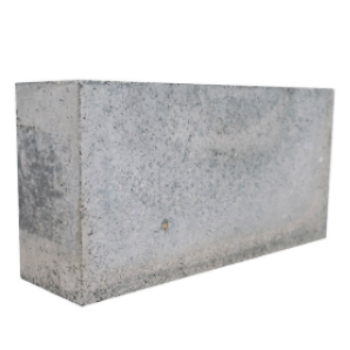
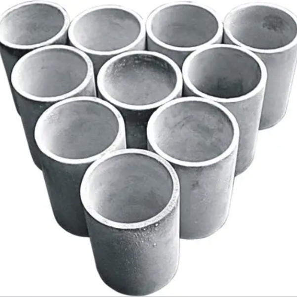
When made right into crucibles– vessels developed to consist of and warmth materials– SiC outshines traditional products like quartz, graphite, and alumina in both life-span and process reliability.
1.2 Microstructure and Mechanical Security
The performance of SiC crucibles is closely connected to their microstructure, which depends upon the manufacturing method and sintering ingredients used.
Refractory-grade crucibles are commonly generated through reaction bonding, where permeable carbon preforms are penetrated with molten silicon, forming β-SiC with the reaction Si(l) + C(s) → SiC(s).
This process yields a composite structure of key SiC with recurring totally free silicon (5– 10%), which boosts thermal conductivity but might limit usage over 1414 ° C(the melting factor of silicon).
Additionally, fully sintered SiC crucibles are made via solid-state or liquid-phase sintering making use of boron and carbon or alumina-yttria additives, accomplishing near-theoretical thickness and higher pureness.
These exhibit superior creep resistance and oxidation stability yet are much more costly and challenging to produce in large sizes.

( Silicon Carbide Crucibles)
The fine-grained, interlacing microstructure of sintered SiC offers excellent resistance to thermal exhaustion and mechanical disintegration, important when dealing with liquified silicon, germanium, or III-V substances in crystal development procedures.
Grain limit design, consisting of the control of second stages and porosity, plays a crucial duty in determining long-term sturdiness under cyclic heating and aggressive chemical atmospheres.
2. Thermal Efficiency and Environmental Resistance
2.1 Thermal Conductivity and Heat Distribution
One of the specifying advantages of SiC crucibles is their high thermal conductivity, which allows rapid and consistent warmth transfer throughout high-temperature handling.
In comparison to low-conductivity products like integrated silica (1– 2 W/(m · K)), SiC successfully disperses thermal energy throughout the crucible wall, lessening localized locations and thermal slopes.
This uniformity is important in processes such as directional solidification of multicrystalline silicon for photovoltaics, where temperature homogeneity straight influences crystal high quality and problem density.
The mix of high conductivity and low thermal growth causes an extremely high thermal shock specification (R = k(1 − ν)α/ σ), making SiC crucibles immune to cracking throughout quick heating or cooling down cycles.
This permits faster heating system ramp prices, boosted throughput, and decreased downtime due to crucible failure.
Furthermore, the material’s capacity to stand up to duplicated thermal biking without substantial destruction makes it suitable for batch handling in commercial heaters operating over 1500 ° C.
2.2 Oxidation and Chemical Compatibility
At elevated temperature levels in air, SiC goes through passive oxidation, creating a safety layer of amorphous silica (SiO ₂) on its surface area: SiC + 3/2 O TWO → SiO ₂ + CO.
This glassy layer densifies at high temperatures, acting as a diffusion barrier that reduces additional oxidation and protects the underlying ceramic structure.
However, in reducing atmospheres or vacuum problems– usual in semiconductor and steel refining– oxidation is suppressed, and SiC remains chemically secure versus molten silicon, aluminum, and numerous slags.
It resists dissolution and reaction with molten silicon approximately 1410 ° C, although prolonged direct exposure can lead to slight carbon pickup or interface roughening.
Crucially, SiC does not introduce metallic pollutants right into sensitive melts, an essential requirement for electronic-grade silicon manufacturing where contamination by Fe, Cu, or Cr should be kept below ppb degrees.
However, treatment has to be taken when refining alkaline planet metals or very responsive oxides, as some can wear away SiC at severe temperature levels.
3. Production Processes and Quality Control
3.1 Construction Techniques and Dimensional Control
The manufacturing of SiC crucibles entails shaping, drying out, and high-temperature sintering or seepage, with techniques chosen based upon needed pureness, size, and application.
Typical creating methods consist of isostatic pushing, extrusion, and slip casting, each using different degrees of dimensional accuracy and microstructural uniformity.
For huge crucibles made use of in photovoltaic ingot spreading, isostatic pushing makes certain consistent wall surface density and density, lowering the risk of crooked thermal expansion and failing.
Reaction-bonded SiC (RBSC) crucibles are affordable and widely used in foundries and solar sectors, though recurring silicon restrictions maximum solution temperature.
Sintered SiC (SSiC) variations, while much more pricey, offer superior purity, stamina, and resistance to chemical strike, making them appropriate for high-value applications like GaAs or InP crystal growth.
Accuracy machining after sintering might be called for to accomplish tight tolerances, specifically for crucibles utilized in vertical slope freeze (VGF) or Czochralski (CZ) systems.
Surface area finishing is important to lessen nucleation sites for problems and make sure smooth thaw flow during casting.
3.2 Quality Control and Efficiency Recognition
Extensive quality control is essential to make certain integrity and long life of SiC crucibles under requiring operational problems.
Non-destructive evaluation techniques such as ultrasonic screening and X-ray tomography are used to discover inner fractures, gaps, or thickness variants.
Chemical analysis via XRF or ICP-MS confirms reduced levels of metallic pollutants, while thermal conductivity and flexural strength are measured to confirm material uniformity.
Crucibles are typically subjected to simulated thermal biking examinations prior to delivery to determine prospective failure modes.
Set traceability and accreditation are common in semiconductor and aerospace supply chains, where part failing can cause pricey manufacturing losses.
4. Applications and Technical Influence
4.1 Semiconductor and Photovoltaic Industries
Silicon carbide crucibles play a crucial role in the production of high-purity silicon for both microelectronics and solar batteries.
In directional solidification furnaces for multicrystalline solar ingots, huge SiC crucibles serve as the main container for molten silicon, withstanding temperatures above 1500 ° C for numerous cycles.
Their chemical inertness protects against contamination, while their thermal security makes certain uniform solidification fronts, causing higher-quality wafers with fewer dislocations and grain limits.
Some manufacturers coat the internal surface with silicon nitride or silica to additionally reduce bond and help with ingot release after cooling down.
In research-scale Czochralski development of compound semiconductors, smaller sized SiC crucibles are made use of to hold thaws of GaAs, InSb, or CdTe, where marginal reactivity and dimensional security are paramount.
4.2 Metallurgy, Factory, and Arising Technologies
Beyond semiconductors, SiC crucibles are crucial in metal refining, alloy preparation, and laboratory-scale melting procedures including light weight aluminum, copper, and precious metals.
Their resistance to thermal shock and disintegration makes them ideal for induction and resistance heating systems in shops, where they outlast graphite and alumina choices by several cycles.
In additive production of reactive metals, SiC containers are used in vacuum cleaner induction melting to stop crucible breakdown and contamination.
Arising applications consist of molten salt reactors and concentrated solar power systems, where SiC vessels might consist of high-temperature salts or liquid metals for thermal energy storage.
With recurring developments in sintering innovation and coating design, SiC crucibles are positioned to support next-generation materials processing, making it possible for cleaner, much more efficient, and scalable industrial thermal systems.
In summary, silicon carbide crucibles stand for a vital enabling modern technology in high-temperature material synthesis, integrating extraordinary thermal, mechanical, and chemical efficiency in a solitary engineered part.
Their prevalent fostering across semiconductor, solar, and metallurgical sectors highlights their function as a cornerstone of modern industrial porcelains.
5. Supplier
Advanced Ceramics founded on October 17, 2012, is a high-tech enterprise committed to the research and development, production, processing, sales and technical services of ceramic relative materials and products. Our products includes but not limited to Boron Carbide Ceramic Products, Boron Nitride Ceramic Products, Silicon Carbide Ceramic Products, Silicon Nitride Ceramic Products, Zirconium Dioxide Ceramic Products, etc. If you are interested, please feel free to contact us.
Tags: Silicon Carbide Crucibles, Silicon Carbide Ceramic, Silicon Carbide Ceramic Crucibles
All articles and pictures are from the Internet. If there are any copyright issues, please contact us in time to delete.
Inquiry us
Error: Contact form not found.