1. Fundamental Duties and Category Frameworks
1.1 Interpretation and Practical Purposes

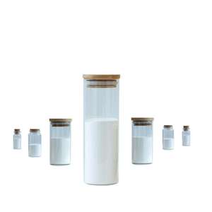
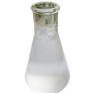
(Concrete Admixtures)
Concrete admixtures are chemical or mineral materials added in small quantities– typically much less than 5% by weight of concrete– to change the fresh and solidified buildings of concrete for specific design demands.
They are presented throughout blending to enhance workability, control setting time, boost resilience, minimize leaks in the structure, or enable sustainable formulations with lower clinker material.
Unlike additional cementitious products (SCMs) such as fly ash or slag, which partly replace concrete and contribute to toughness development, admixtures primarily work as efficiency modifiers as opposed to architectural binders.
Their specific dosage and compatibility with cement chemistry make them indispensable devices in contemporary concrete modern technology, especially in complicated construction jobs entailing long-distance transport, high-rise pumping, or extreme environmental direct exposure.
The performance of an admixture depends on variables such as concrete structure, water-to-cement proportion, temperature, and mixing treatment, necessitating mindful option and screening prior to field application.
1.2 Broad Categories Based on Feature
Admixtures are generally classified right into water reducers, set controllers, air entrainers, specialized additives, and hybrid systems that integrate numerous functionalities.
Water-reducing admixtures, consisting of plasticizers and superplasticizers, disperse concrete bits with electrostatic or steric repulsion, boosting fluidity without enhancing water web content.
Set-modifying admixtures include accelerators, which reduce establishing time for cold-weather concreting, and retarders, which postpone hydration to stop cold joints in huge pours.
Air-entraining agents present tiny air bubbles (10– 1000 µm) that enhance freeze-thaw resistance by giving pressure relief throughout water growth.
Specialty admixtures incorporate a large range, consisting of deterioration preventions, contraction reducers, pumping aids, waterproofing agents, and viscosity modifiers for self-consolidating concrete (SCC).
Extra lately, multi-functional admixtures have emerged, such as shrinkage-compensating systems that combine extensive representatives with water reduction, or inner healing agents that release water over time to reduce autogenous contraction.
2. Chemical Mechanisms and Product Communications
2.1 Water-Reducing and Dispersing Professionals
One of the most widely made use of chemical admixtures are high-range water reducers (HRWRs), frequently referred to as superplasticizers, which come from families such as sulfonated naphthalene formaldehyde (SNF), melamine formaldehyde (SMF), and polycarboxylate ethers (PCEs).
PCEs, one of the most sophisticated class, function via steric obstacle: their comb-like polymer chains adsorb onto concrete particles, producing a physical obstacle that prevents flocculation and keeps dispersion.
( Concrete Admixtures)
This enables considerable water reduction (as much as 40%) while preserving high slump, enabling the manufacturing of high-strength concrete (HSC) and ultra-high-performance concrete (UHPC) with compressive strengths exceeding 150 MPa.
Plasticizers like SNF and SMF operate primarily through electrostatic repulsion by enhancing the adverse zeta possibility of cement bits, though they are much less reliable at low water-cement ratios and much more sensitive to dosage restrictions.
Compatibility between superplasticizers and concrete is critical; variants in sulfate web content, alkali levels, or C ₃ A (tricalcium aluminate) can bring about quick depression loss or overdosing impacts.
2.2 Hydration Control and Dimensional Stability
Increasing admixtures, such as calcium chloride (though limited as a result of corrosion risks), triethanolamine (TEA), or soluble silicates, promote early hydration by boosting ion dissolution rates or creating nucleation websites for calcium silicate hydrate (C-S-H) gel.
They are crucial in cool climates where reduced temperatures slow down setting and rise formwork removal time.
Retarders, including hydroxycarboxylic acids (e.g., citric acid, gluconate), sugars, and phosphonates, feature by chelating calcium ions or creating protective movies on cement grains, delaying the start of tensing.
This extended workability window is important for mass concrete positionings, such as dams or foundations, where warm build-up and thermal splitting need to be managed.
Shrinkage-reducing admixtures (SRAs) are surfactants that reduced the surface area stress of pore water, reducing capillary tensions during drying and minimizing fracture formation.
Large admixtures, typically based on calcium sulfoaluminate (CSA) or magnesium oxide (MgO), generate regulated development during curing to balance out drying contraction, commonly used in post-tensioned slabs and jointless floors.
3. Longevity Improvement and Ecological Adaptation
3.1 Defense Versus Ecological Deterioration
Concrete revealed to harsh atmospheres advantages considerably from specialized admixtures made to withstand chemical strike, chloride ingress, and reinforcement corrosion.
Corrosion-inhibiting admixtures include nitrites, amines, and organic esters that develop easy layers on steel rebars or reduce the effects of hostile ions.
Movement preventions, such as vapor-phase preventions, diffuse via the pore structure to safeguard embedded steel even in carbonated or chloride-contaminated areas.
Waterproofing and hydrophobic admixtures, including silanes, siloxanes, and stearates, reduce water absorption by changing pore surface area power, boosting resistance to freeze-thaw cycles and sulfate attack.
Viscosity-modifying admixtures (VMAs) enhance communication in undersea concrete or lean mixes, stopping segregation and washout during positioning.
Pumping aids, usually polysaccharide-based, decrease friction and enhance circulation in long delivery lines, decreasing energy intake and endure equipment.
3.2 Inner Treating and Long-Term Performance
In high-performance and low-permeability concretes, autogenous contraction ends up being a significant concern because of self-desiccation as hydration profits without external water system.
Interior healing admixtures resolve this by integrating light-weight accumulations (e.g., expanded clay or shale), superabsorbent polymers (SAPs), or pre-wetted permeable carriers that release water progressively into the matrix.
This sustained wetness schedule advertises total hydration, reduces microcracking, and improves long-lasting toughness and sturdiness.
Such systems are especially effective in bridge decks, tunnel cellular linings, and nuclear containment frameworks where life span goes beyond 100 years.
Additionally, crystalline waterproofing admixtures respond with water and unhydrated concrete to develop insoluble crystals that block capillary pores, providing long-term self-sealing capacity even after breaking.
4. Sustainability and Next-Generation Innovations
4.1 Allowing Low-Carbon Concrete Technologies
Admixtures play an essential duty in decreasing the ecological footprint of concrete by enabling higher substitute of Rose city cement with SCMs like fly ash, slag, and calcined clay.
Water reducers permit lower water-cement proportions despite slower-reacting SCMs, making certain adequate stamina development and longevity.
Establish modulators compensate for postponed setup times connected with high-volume SCMs, making them viable in fast-track construction.
Carbon-capture admixtures are emerging, which assist in the direct consolidation of CO two into the concrete matrix throughout blending, converting it into secure carbonate minerals that boost very early strength.
These modern technologies not only minimize personified carbon but additionally improve performance, aligning economic and ecological objectives.
4.2 Smart and Adaptive Admixture Solutions
Future developments consist of stimuli-responsive admixtures that release their energetic elements in response to pH changes, moisture levels, or mechanical damages.
Self-healing concrete includes microcapsules or bacteria-laden admixtures that activate upon split development, speeding up calcite to seal crevices autonomously.
Nanomodified admixtures, such as nano-silica or nano-clay dispersions, improve nucleation thickness and refine pore structure at the nanoscale, dramatically boosting stamina and impermeability.
Digital admixture dosing systems making use of real-time rheometers and AI algorithms enhance mix performance on-site, lessening waste and variability.
As framework demands grow for durability, long life, and sustainability, concrete admixtures will certainly remain at the leading edge of product development, changing a centuries-old compound into a clever, flexible, and environmentally responsible construction tool.
5. Supplier
Cabr-Concrete is a supplier of Concrete Admixture under TRUNNANO, with over 12 years of experience in nano-building energy conservation and nanotechnology development. It accepts payment via Credit Card, T/T, West Union and Paypal. TRUNNANO will ship the goods to customers overseas through FedEx, DHL, by air, or by sea. If you are looking for high quality Concrete Admixture, please feel free to contact us and send an inquiry.
Tags: concrete additives, concrete admixture, Lightweight Concrete Admixtures
All articles and pictures are from the Internet. If there are any copyright issues, please contact us in time to delete.
Inquiry us
Error: Contact form not found.