1. hemical Nature and Architectural Characteristics
1.1 Molecular Structure and Self-Assembly Behavior

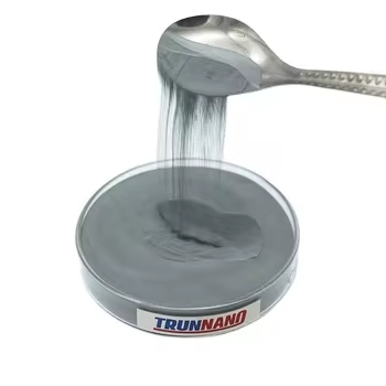
(Calcium Stearate Powder)
Calcium stearate powder is a metallic soap developed by the neutralization of stearic acid– a C18 saturated fatty acid– with calcium hydroxide or calcium oxide, producing the chemical formula Ca(C ₁₈ H ₃₅ O ₂)TWO.
This substance belongs to the wider course of alkali planet metal soaps, which exhibit amphiphilic buildings because of their twin molecular architecture: a polar, ionic “head” (the calcium ion) and 2 long, nonpolar hydrocarbon “tails” derived from stearic acid chains.
In the solid state, these molecules self-assemble right into split lamellar frameworks through van der Waals communications in between the hydrophobic tails, while the ionic calcium facilities provide structural cohesion through electrostatic pressures.
This distinct arrangement underpins its functionality as both a water-repellent agent and a lubricant, enabling performance throughout varied material systems.
The crystalline kind of calcium stearate is usually monoclinic or triclinic, depending on processing conditions, and exhibits thermal stability approximately around 150– 200 ° C prior to decomposition begins.
Its reduced solubility in water and most organic solvents makes it especially appropriate for applications calling for consistent surface area alteration without seeping.
1.2 Synthesis Pathways and Industrial Production Techniques
Commercially, calcium stearate is generated via 2 main courses: straight saponification and metathesis response.
In the saponification procedure, stearic acid is responded with calcium hydroxide in a liquid medium under controlled temperature (usually 80– 100 ° C), adhered to by purification, washing, and spray drying out to generate a fine, free-flowing powder.
Conversely, metathesis involves responding sodium stearate with a soluble calcium salt such as calcium chloride, speeding up calcium stearate while generating salt chloride as a byproduct, which is after that eliminated via substantial rinsing.
The option of technique influences particle size distribution, purity, and recurring dampness material– essential parameters influencing efficiency in end-use applications.
High-purity qualities, particularly those meant for pharmaceuticals or food-contact products, go through extra filtration actions to fulfill governing requirements such as FCC (Food Chemicals Codex) or USP (United States Pharmacopeia).
( Calcium Stearate Powder)
Modern manufacturing facilities use continuous activators and automated drying out systems to make sure batch-to-batch uniformity and scalability.
2. Practical Functions and Mechanisms in Material Systems
2.1 Interior and Outside Lubrication in Polymer Handling
Among one of the most crucial features of calcium stearate is as a multifunctional lube in thermoplastic and thermoset polymer production.
As an internal lube, it minimizes thaw viscosity by hindering intermolecular friction between polymer chains, assisting in much easier flow throughout extrusion, injection molding, and calendaring processes.
At the same time, as an exterior lubricating substance, it moves to the surface area of liquified polymers and develops a thin, release-promoting film at the user interface between the product and processing devices.
This double action decreases die buildup, avoids staying with molds, and enhances surface area coating, thus improving manufacturing performance and product top quality.
Its efficiency is particularly remarkable in polyvinyl chloride (PVC), where it also contributes to thermal stability by scavenging hydrogen chloride launched throughout degradation.
Unlike some synthetic lubes, calcium stearate is thermally secure within common processing home windows and does not volatilize too soon, making sure consistent performance throughout the cycle.
2.2 Water Repellency and Anti-Caking Properties
As a result of its hydrophobic nature, calcium stearate is extensively employed as a waterproofing agent in construction products such as cement, plaster, and plasters.
When integrated into these matrices, it lines up at pore surface areas, decreasing capillary absorption and enhancing resistance to moisture ingress without dramatically changing mechanical stamina.
In powdered products– including plant foods, food powders, pharmaceuticals, and pigments– it functions as an anti-caking agent by layer private bits and preventing load brought on by humidity-induced connecting.
This enhances flowability, dealing with, and dosing accuracy, specifically in computerized product packaging and blending systems.
The device depends on the formation of a physical barrier that hinders hygroscopic uptake and reduces interparticle adhesion forces.
Since it is chemically inert under normal storage conditions, it does not respond with active ingredients, maintaining service life and performance.
3. Application Domains Across Industries
3.1 Duty in Plastics, Rubber, and Elastomer Manufacturing
Beyond lubrication, calcium stearate serves as a mold release agent and acid scavenger in rubber vulcanization and synthetic elastomer production.
Throughout compounding, it makes certain smooth脱模 (demolding) and secures pricey metal passes away from rust caused by acidic byproducts.
In polyolefins such as polyethylene and polypropylene, it enhances dispersion of fillers like calcium carbonate and talc, adding to uniform composite morphology.
Its compatibility with a wide variety of ingredients makes it a preferred part in masterbatch formulations.
Furthermore, in eco-friendly plastics, where conventional lubricants may interfere with deterioration pathways, calcium stearate supplies a more ecologically suitable choice.
3.2 Usage in Pharmaceuticals, Cosmetics, and Food Products
In the pharmaceutical industry, calcium stearate is frequently utilized as a glidant and lubricant in tablet compression, ensuring constant powder circulation and ejection from strikes.
It prevents sticking and capping problems, directly affecting manufacturing yield and dose harmony.
Although occasionally confused with magnesium stearate, calcium stearate is favored in particular solutions because of its greater thermal security and reduced capacity for bioavailability interference.
In cosmetics, it works as a bulking agent, structure modifier, and emulsion stabilizer in powders, foundations, and lipsticks, providing a smooth, silky feeling.
As a food additive (E470(ii)), it is authorized in several territories as an anticaking agent in dried out milk, flavors, and cooking powders, adhering to strict restrictions on optimum allowed concentrations.
Governing compliance needs extensive control over heavy steel material, microbial lots, and recurring solvents.
4. Security, Environmental Impact, and Future Overview
4.1 Toxicological Account and Regulatory Condition
Calcium stearate is usually acknowledged as secure (GRAS) by the united state FDA when used according to great manufacturing methods.
It is badly soaked up in the stomach system and is metabolized right into normally taking place fats and calcium ions, both of which are physiologically manageable.
No significant proof of carcinogenicity, mutagenicity, or reproductive poisoning has actually been reported in conventional toxicological research studies.
Nevertheless, inhalation of great powders during commercial handling can trigger breathing inflammation, demanding ideal air flow and individual protective devices.
Environmental impact is minimal due to its biodegradability under cardio problems and low aquatic toxicity.
4.2 Arising Patterns and Sustainable Alternatives
With boosting emphasis on eco-friendly chemistry, research is focusing on bio-based production paths and decreased ecological impact in synthesis.
Efforts are underway to acquire stearic acid from eco-friendly sources such as hand bit or tallow, improving lifecycle sustainability.
Additionally, nanostructured types of calcium stearate are being discovered for boosted diffusion effectiveness at lower does, possibly decreasing overall material use.
Functionalization with various other ions or co-processing with natural waxes may expand its utility in specialized layers and controlled-release systems.
In conclusion, calcium stearate powder exemplifies just how a straightforward organometallic substance can play a disproportionately large role across commercial, consumer, and healthcare fields.
Its combination of lubricity, hydrophobicity, chemical stability, and governing reputation makes it a keystone additive in modern formula scientific research.
As industries remain to demand multifunctional, safe, and lasting excipients, calcium stearate continues to be a benchmark product with sustaining significance and developing applications.
5. Vendor
RBOSCHCO is a trusted global chemical material supplier & manufacturer with over 12 years experience in providing super high-quality chemicals and Nanomaterials. The company export to many countries, such as USA, Canada, Europe, UAE, South Africa, Tanzania, Kenya, Egypt, Nigeria, Cameroon, Uganda, Turkey, Mexico, Azerbaijan, Belgium, Cyprus, Czech Republic, Brazil, Chile, Argentina, Dubai, Japan, Korea, Vietnam, Thailand, Malaysia, Indonesia, Australia,Germany, France, Italy, Portugal etc. As a leading nanotechnology development manufacturer, RBOSCHCO dominates the market. Our professional work team provides perfect solutions to help improve the efficiency of various industries, create value, and easily cope with various challenges. If you are looking for baerlocher calcium stearate, please feel free to contact us and send an inquiry.
Tags: Calcium Stearate Powder, calcium stearate,ca stearate
All articles and pictures are from the Internet. If there are any copyright issues, please contact us in time to delete.
Inquiry us
Error: Contact form not found.